Read The Amazing Story of Quantum Mechanics Online
Authors: James Kakalios
The Amazing Story of Quantum Mechanics (32 page)

BOOK: The Amazing Story of Quantum Mechanics
3.2Mb size Format: txt, pdf, ePub
ads
LEDs back in the 1960s could produce only red light at very low intensity. In the past thirty years the luminosity of these devices has increased by a factor of ten thousand, and LEDs that generate white light can put out as much illumination as an incandescent 60-watt lightbulb. LEDs are much longer-lived than standard incandescent bulbs, and some LEDs manufactured in the 1970s and 1980s are still operational today. There is interest in replacing silicon in these devices with organic chemicals as the semiconductor material since these organic light-emitting diodes (OLEDs) can be spread easily over large areas and in some cases are brighter than silicon-based LEDs. These devices use polymers consisting of long chains of carbon atoms bonded in a line, with different chemical groups protruding from the chain (referred to by chemists as “organic molecules”) as the semiconductor element in the LED. There may come a day, and it may be relatively soon, when conventional incandescent lightbulbs are replaced with white-light LEDs, which are more environmentally friendly, use less power, and last much longer than compact fluorescent bulbs. All thanks to quantum mechanics.
If you’ll allow me to digress, Fearless Reader, I’d like to relate a personal experience with diodes. When I was a new graduate student, I had a desk in the research group where I would eventually conduct my dissertation studies. A more senior student, Peter, had recently convinced our research adviser to install a separate phone line in the lab where Peter worked. This was back in the days before AT&T had been broken up into the “Baby Bells” by court order, and one had to order phones from Bell Telephone, which would then come and install the landline (cell phones were an extreme rarity back then). As a cost-saving measure, our professor had ordered a phone that would allow incoming calls but not outgoing ones. As soon as the phone company employees departed, Peter took the phone off the wall, opened it up, and compared it carefully to another phone that did allow outgoing calls. At one key juncture Peter noted—a diode! A simple and elegant way to ensure that signals could propagate in one direction but not in the other. Removing this semiconductor device and reconnecting the wires, Peter was then able to make outgoing calls on the phone.
All of which I was unaware of when the next day, a Saturday, the phone company employees returned to check on the line and attach the sticker to the phone that would indicate its assigned phone number. A short while later the phone in the common room where I was studying rang, and when I answered it, the telephone workers apologized, saying that they just wanted to make sure that the phone could make outgoing calls. A short while after they left, Peter came in and told me about his “fixing” of the phone in his lab. He turned white when I mentioned that the phone company men had been by earlier, wanting to make sure the phone could make as well as receive calls. Racing to his lab, he quickly ascertained that the phone would no longer make calls. I watched as he took the phone off the wall, removed the plastic cover, and spotted a small white card
inside
the phone, tucked underneath a tangle of wires. Removing the card with tweezers, we saw the handwritten suggestion: “Try it now, whiz kid.”
inside
the phone, tucked underneath a tangle of wires. Removing the card with tweezers, we saw the handwritten suggestion: “Try it now, whiz kid.”
Sure enough, the phone had been completely rewired, with great effort going into replicating the functions performed by one simple diode. Without the innovation of the solid-state diode, electronics would be a great deal more complicated and bulkier—though the phone company would still always win in the end!
CHAPTER SEVENTEEN
Big Changes Come in Small Packages
The diode was the first important
step into the semiconductor age, and the second major advance also came from Bell Labs, with the invention of the transistor. There are two different structures for a transistor—one that involves adding another n-type semiconductor to the pn junction (to make an npn device) and the simpler-to-understand (in my opinion) field-effect device. I discuss here the field-effect structure, as it will also help us understand how a flash memory stick (also known as a jump drive or a USB drive) works.
step into the semiconductor age, and the second major advance also came from Bell Labs, with the invention of the transistor. There are two different structures for a transistor—one that involves adding another n-type semiconductor to the pn junction (to make an npn device) and the simpler-to-understand (in my opinion) field-effect device. I discuss here the field-effect structure, as it will also help us understand how a flash memory stick (also known as a jump drive or a USB drive) works.
The arguments here do not depend on whether the material is n-type or p-type, but for simplicity we will pick a p-type semiconductor for definiteness. Imagine a semiconductor, such as silicon, as a rectangular slab, longer and wider than it is thick, as illustrated in Figure 44a. On part of the top of the semiconductor we place an insulator that could be silicon dioxide, which in its crystalline form is called “quartz” and in an amorphous phase is termed “glass.” On the top of the semiconductor surface there are two metal electrodes at each end, not touching the insulator. At one electrode a voltage is applied, and the resulting current pushed through the semiconductor is withdrawn at the other electrode. So far we have just described a way to measure the current passing through the material for a given applied voltage, and the insulator plays no role in the conduction through the semiconductor. The metal electrodes on either side of the insulator have a surfeit of free electrons, and where they are in electrical contact with the p-type semiconductor they form an effective p-n junction. If we are trying to flow electrons through a p-type doped material these back-to-back p-n junctions will make it very difficult for the current to move through the semiconductor. Now, to make this device a transistor, let’s put a sheet of metal atop the insulating slab. As shown in Figure 44a, there are two metal electrodes apart from each other on the top of the semiconductor, between which is an insulating slab, atop of which is another metal electrode. We have constructed a field-effect transistor.
66
66
What happens if we apply a positive voltage to the metal electrode that is covering the insulating slab? As this top metal electrode is in contact with an insulator that does not conduct electricity, the charges will just stay on the metal, having no place to go. The electric field created by these charges will extend through the insulator into the semiconductor layer. Compared to the insulator, the semiconductor beneath the insulating slab is a pretty good conductor, though not as good as the metal. Electrons will be drawn toward the region near the insulator-semiconductor interface by the electric field. Without a voltage, the metal is electrically neutral, and there is no reason for any electrons in the semiconductor to be pulled toward this region. With a voltage applied to the insulator, piling up positive charges on the top of the insulating slab, a channel of electrons connecting the two other metal electrodes at either end of the semiconductor is created, shown in Figure 44b. This has the effect of reducing the electric field at each pn junction where the metal electrodes contact the semiconductor, and the ability of the material to carry a flow of electrons will be greatly improved. The positive voltage on the metal atop the insulator in a sense opens a gate through which the electrons can flow. Applying a negative voltage would push electrons away from the insulator-semiconductor interface, and the ability for electrons to flow would be reduced (the gate would swing shut in this case). This is what a transistor does—it provides a way, by applying a small voltage to the gate electrode, to dramatically alter and potentially amplify a current passing through the semiconductor.
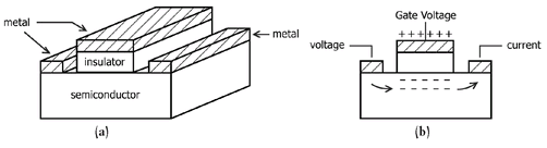
Figure 44:
Sketch of a simple transistor device structure (a). Two metal electrodes on the top of the semiconductor are used to pass a current through the device. A thin insulator (such as glass), on which is a metal electrode, lies on top of the semiconductor between the two metal electrodes used to pass the current. When a positive voltage is applied to the “gate electrode,” positive charges accumulate on the top of the insulator, which attract electrons in the semiconductor to the region underneath the insulator (b). These electrons improve the ability of the semiconductor to pass a current between the two metal electrodes, and the current is made much larger by the application of the “gate voltage.”
Sketch of a simple transistor device structure (a). Two metal electrodes on the top of the semiconductor are used to pass a current through the device. A thin insulator (such as glass), on which is a metal electrode, lies on top of the semiconductor between the two metal electrodes used to pass the current. When a positive voltage is applied to the “gate electrode,” positive charges accumulate on the top of the insulator, which attract electrons in the semiconductor to the region underneath the insulator (b). These electrons improve the ability of the semiconductor to pass a current between the two metal electrodes, and the current is made much larger by the application of the “gate voltage.”
Remember from the last chapter the discussion of the influence of a built-in electric field on a pn junction on the energy of the bands of states in a semiconductor. Changing the electric field alters the energy of the quantum states that are calculated using the Schrödinger equation (demonstrated through the influence of the electric field of the positively charged nucleus on the electrons’ allowed energies). If no voltage is applied, then there is no extra field on the semiconductor, and the number of electrons available to flow in the p-type semiconductor is very low. If a positive voltage is applied to the insulator, it will change the energy of both the orchestra and balcony of states. The change is strongest near the positive charges on the insulator and decreases as one goes farther into the semiconductor. Near the region by the insulator, electrons can now be thermally promoted into the balcony of the material. Consequently, the region near the insulator, when there is a positive voltage applied to a p-type semiconductor, will see a large enhancement in its ability to carry a current of electrons. The sensitivity of the current passing through this device to an externally applied gate voltage results from changes in the energy of the quantum states in the filled orchestra and empty balcony, which in turn are understood from the quantum theory of solids.
If the voltage applied to the insulator changes with time (such as in the case of a weak radio signal detected by an antenna), then the current passing through the semiconductor will also vary in time but as an amplified version, capable of driving speakers so that the radio signal can be heard. Transistor radios and television sets, employing the amplification capability of these devices, were some of the first applications of these devices, replacing the vacuum tubes and making these consumer electronic products smaller and lighter.
Vacuum tubes accomplish the same task as a transistor, by heating a wire until electrons “boil off” the filament. A voltage applied to a screen then attracts these free electrons to a collector, and depending on the voltage, the electrons can be accelerated toward or reflected away from the collector. In order to minimize the electron beam’s scattering from air molecules, all the air in the tube should be removed. Such devices are bulky and fragile, use considerable power, generate a great deal of heat (necessitating spacing them a distance from each other), and are expensive to produce. A semiconductor transistor accomplishes the same task without requiring a glass-enclosed vacuum, in a compact, rugged design, and wastes very little energy as heat; and the only limitations on the size of the device are the ingenuity in constructing the insulating slab and applying the metal electrodes, and making contact with the rest of the circuit.
If we can make the transistors small, we can put several transistors on a single piece of silicon. By varying the concentration of chemical impurities that add either excess electrons or holes to the semiconductor, and through the placement of other metal electrodes and insulating slabs, one can incorporate diodes, resistors, and capacitors into the same semiconductor along with the transistor. In this way the various aspects of a complex circuit can be integrated onto a single semiconductor chip. In 1958, just a year after the Challengers of the Unknown faced off against ULTIVAC, whose electronic brain was as large as a room (Figure 39), Robert Noyce and Jack Kilby independently designed and constructed the first integrated circuits. The first of these devices incorporated roughly five to ten transistors on a single silicon wafer. In the introduction I discussed Moore’s law, whereby the number of transistors on an integrated circuit doubles every two years. The continued accuracy of this prediction surprised even Moore, and in 2010 the number of transistors on a chip can be over a billion. Estimates of the number of transistors in a computer’s microprocessor suggest that on a typical college campus there are many more transistors than there are stars in the Milky Way.
These transistors do more than simply amplify information, as in the case of a weak electromagnetic wave signal being boosted in a cell phone. They also can store and manipulate information. When a large positive voltage is applied to the gate electrode on the insulator, the current-carrying capability of the semiconductor is greatly enhanced. Removing this large voltage restores the silicon to its poorly conducting state. The first situation can be described as a “one,” while the second is a “zero.” Just as the DVDs and CDs in the previous chapter are able to encode complex information through a series of ones and zeros, the transistors on the integrated circuits can do the same. However, transistors offer the possibility of much greater sensitivity to small perturbations. Transistors have been fabricated in the research laboratory with dimensions of under a hundred nanometers, where, depending on the voltage applied to the gate electrode, the transport of a single electron can be detected. Computers use transistors as logic elements that can be in an “on” or “off” state—and transistors can be fabricated whereby the difference between the two conditions is the motion of one electron.
BOOK: The Amazing Story of Quantum Mechanics
3.2Mb size Format: txt, pdf, ePub
ads
Other books
Anne Barbour by Point Non Plus nodrm
The Gypsy Morph by Terry Brooks
Motion to Dismiss by Jonnie Jacobs
Lovely by Strider, Jez
Starting from Scratch by Marie Ferrarella
The Mystery of the Fire Dragon by Carolyn Keene
The Curse of the Campfire Weenies by David Lubar
Remember by Mihai, Cristian
Brilliant by Rachel Vail
2 The Dante Connection by Estelle Ryan