Make: Electronics (47 page)
Authors: Charles Platt

Fundamentals
Why the 555 is useful
In its monostable mode (which is what you just saw), the 555 will emit a single pulse of fixed (but programmable) length. Can you imagine some applications? Think in terms of the pulse from the 555 controlling some other component. A motion sensor on an outdoor light, perhaps. When an infra-red detector “sees” something moving, the light comes on for a specific period—which can be controlled by a 555.
Another application could be a toaster. When someone lowers a slice of bread, a switch will close that triggers the toasting cycle. To change the length of the cycle, you could use a potentiometer instead of R4 and attach it to the external lever that determines how dark you want your toast. At the end of the toasting cycle, the output from the 555 would pass through a power transistor, to activate a solenoid (which is like a relay, except that it has no switch contacts) to release the toast.
Intermittent windshield wipers could be controlled by a 555 timer—and on earlier models of cars, they actually were. And what about the burglar alarm that was described at the end of
Chapter 3
? One of the features that I listed, which has not been implemented yet, is that it should shut itself off after a fixed interval. We can use the change of output from a 555 timer to do that.
The experiment that you just performed seemed trivial, but really it implies all kinds of possibilities.
555 timer limits
1.
The timer can run from a stable voltage source ranging from 5 to 15 volts.
2.
Most manufacturers recommend a range from 1K to 1M for the resistor attached to pin 7.
3.
The capacitor value can go as high as you like, if you want to time really long intervals, but the accuracy of the timer will diminish.
4.
The output can deliver as much as 100mA at 9 volts. This is sufficient for a small relay or miniature loudspeaker, as you’ll see in the next experiment.
 Beware of Pin-Shuffling!
In all of the schematics in this book, I’ll show chips as you’d see them from above, with pin 1 at top left. Other schematics that you may see, on websites or in other books, may do things differently. For convenience in drawing circuits, people shuffle the pin numbers on a chip so that pin 1 isn’t necessarily shown adjacent to pin 2.
Look at the schematic in Figure 4-20 and compare it with the one in Figure 4-15. The connections are the same, but the one in Figure 4-20 groups pins to reduce the apparent complexity of the wiring.
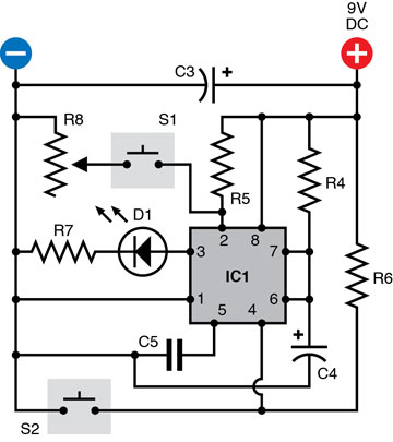
Figure 4-20.
Many people draw schematics in which the pin numbers on a chip are shuffled around to make the schematic smaller or simpler. This is not helpful when you try to build the circuit. The schematic here is for the same circuit as in Figure 4-15. This version would be harder to recreate on a breadboard.
“Pin shuffling” is common because circuit-drawing software tends to do it, and on larger chips, it is necessary for functional clarity of the schematic (i.e., logical groupings of pin names versus physical groupings on memory chips, for example). When you’re first learning to use chips, I think it’s easier to understand a schematic that shows the pins in their actual positions. So that’s the practice I will be using here.
Experiment 17: Set Your Tone
I’m going to show you two other ways in which the 555 timer can be used.
You will need the same items as in
Experiment 16
, plus:
- Additional 555 timer chip. Quantity: 1.
- Miniature loudspeaker. Quantity: 1.
- 100K linear potentiometer. Quantity: 1.
Procedure
Leave the components from
Experiment 16
where they are on the breadboard, and add the next section below them, as shown in Figures 4-21 and 4-22. Resistor R2 is inserted between pins 6 and 7, instead of the jumper wire that shorted the pins together in the previous circuit, and there’s no external input to pin 2 anymore. Instead, pin 2 is connected via a jumper wire to pin 6. The easiest way to do this is by running the wire across the top of the chip.
I have omitted the smoothing capacitor from the schematic in Figure 4-22, because I’m assuming that you’re running this circuit on the same breadboard as the first, where the previous smoothing capacitor is still active.
A loudspeaker in series with a 100Ω resistor (R3) has been substituted for the LED to show the output from the chip. Pin 4, the reset, is disabled by connecting it to the positive voltage supply, as I’m not expecting to use the reset function in this circuit.
Now what happens when you apply power? Immediately, you should hear noise through the loudspeaker. If you don’t hear anything, you almost certainly made a wiring error.
Notice that you don’t have to trigger the chip with a pushbutton anymore. The reason is that when C1 charges and discharges, its fluctuating voltage is connected via a jumper wire across the top of the chip to pin 2, the trigger. In this way, the 555 timer now triggers itself. I’ll describe this in more detail in the next section “Theory: Inside the 555 timer: astable mode,” if you want to see exactly what is going on.
In this mode, the chip is “astable,” meaning that it is not stable, because it flips to and fro endlessly, sending a stream of pulses for as long as the power is connected. The pulses are so rapid that the loudspeaker reproduces them as noise.
In fact, with the component values that I specified for R1, R2, and C1, the 555 chip is emitting about 1,500 pulses per second. In other words, it creates a 1.5 KHz tone.
Check the table on
page 166
to see how different values for R2 and C1 can create different pulse frequencies with the chip in this astable mode. Note that the table assumes a fixed value of 1K for R1!
Figure 4-21.
These components should be added on the same breadboard below the components shown in Figure 4-14. Use the following values to test the 555 timer in its astable mode:
R1: 1K
R2: 10K
R3: 100Ω
C1: 0.047 µF ceramic or electrolytic
C2: 0.1 µF ceramic
IC2: 555 timer
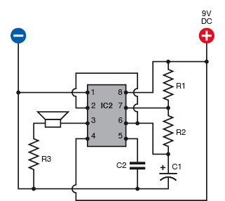
Figure 4-22.
This is the schematic version of the circuit shown in Figure 4-21. The component values are the same.
Theory
Inside the 555 timer: astable mode
Here’s what is happening now, illustrated in Figure 4-23. Initially, the flip-flop grounds C1 as before. But now the low voltage on the capacitor is connected from pin 7 to pin 2 through an external wire. The low voltage tells the chip to trigger itself. The flip-flop obediently flips to its “on” position and sends a positive pulse to the loudspeaker, while removing the negative voltage from pin 7.

Figure 4-23.
When the 555 timer is used in astable mode, resistor R2 is placed between pin 6 and pin 7, and pin 6 is connected via an external wire to pin 2, so that the timer triggers itself.
Now C1 starts charging, as it did when the timer was in monostable mode, except that it is being charged through R1 + R2 in series. Because the resistors have low values, and C1 is also small, C1 charges quickly. When it reaches 2/3 full voltage, comparator B takes action as before, discharging the capacitor and ending the output pulse from pin 3.
The capacitor takes longer to discharge than before, because R2 has been inserted between it and pin 7, the discharge pin. While the capacitor is discharging, its voltage diminishes, and is still linked to pin 2. When the voltage drops to 1/3 of full power or less, comparator A kicks in and sends another pulse to the flip-flop, starting the process all over again.
Summing up:
1.
In astable mode, as soon as power is connected, the flip-flop pulls down the voltage on pin 2, triggering comparator A, which flips the flip-flop to its “down” position.
2.
Pin 3, the output, goes high. The capacitor charges through R1 and R2 in series.
3.
When the capacitor reaches 2/3 of supply voltage, the flip-flop goes “up” and the output at pin 3 goes low. The capacitor starts to discharge through R2.
4.
When the charge on the capacitor diminishes to 1/3 of full voltage, the pull-down on pin 2 flips the flip-flop again and the cycle repeats.
Unequal on/off cycles
When the timer is running in astable mode, C1 charges through R1 and R2 in series. But when C1 discharges, it dumps its voltage through R2 only. This means that the capacitor charges more slowly than it discharges. While it is charging, the output on pin 3 is high; while it is discharging, the output on pin 3 is low. Consequently the “on” cycle is always longer than the “off” cycle. Figure 4-24 shows this as a simple graph.
If you want the on and off cycles to be equal, or if you want to adjust the on and off cycles independently (for example, because you want to send a very brief pulse to another chip, followed by a longer gap until the next pulse), all you need to do is add a diode, as shown in Figure 4-25.
Now when C1 charges, the electricity flows through R1 as before but takes a shortcut around R2, through diode D1. When C1 discharges, the diode blocks the flow of electricity in that direction, and so the discharge goes back through R2.